|
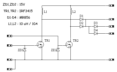
Electromagnetic Pistol: CS-P01A Voltage Converter Construction The space allocated for the boost converter allows for a maximum board size of 55 mm x 48 mm. The circuit design (fig 1) for the dual boost converter was entered into a PCB design package (Electronic Design Studio 3) and the PCB components arranged so that a minimum number of wire link jumpers were necessary. Height restrictions demanded that the inductors had to be placed along the centre line of the board. Fig 2shows a screen shot of the final EDS design.
Fig 1. Schematic of dual boost converter.
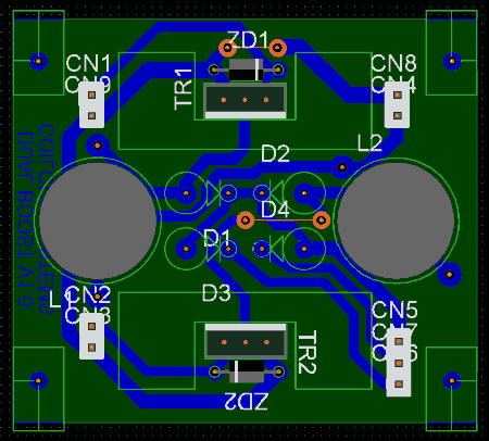
Fig 2. Component layout.
The orange pads and lines represent wire links on the component side of the board.. The circuit was printed on a sheet of tracing paper (fig 3.) and a piece of 'fotoboard' was exposed in a UV light box for about 100 seconds. After exposure the board was treated with developer solution and then etched in a ferric chloride bath (lovely stuff ;-)).
Fig 3. Positive image of PCB tracks.
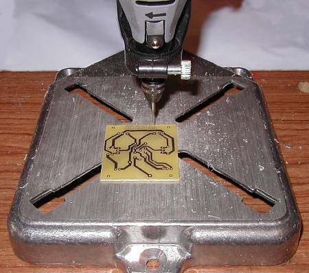
The next job was to drill the pin holes in the board. It's possible to use a hand drill and standard HSS 'Jobber' drill bits to make a PCB but it can be a very tedious task. Some sort of drill press makes life a whole lot easier. Tungsten carbide drill bits are also better if there are lots of holes to drill (the glass fibre board quickly blunts HSS). Fig 4 shows the Dremel drill and press I use for making PCBs.
Fig 4. Dremel drill press for PCB manufacture.
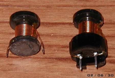
The inductors needed to be modified due to the height restriction mentioned above. Fig 5 shows the removal of the inductor base (it was a well glued in place).
Fig 5. Removal of inductor base mount to reduce overall height.
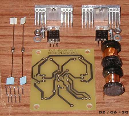
Finally the components were gathered together and soldered into place. Fig 6 illustrates the components (except for the output diodes). The heatsinks are not standard parts, they were made from a CPU heatsink.
Fig 6. Components ready for assembly (forgot the output diodes!).
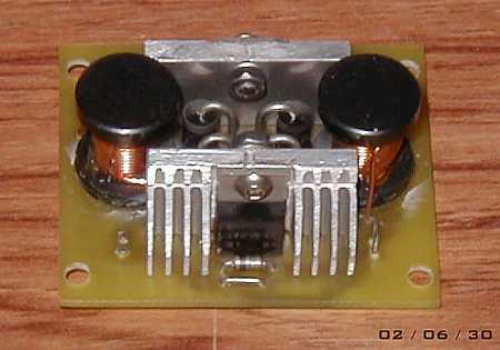
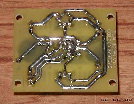
Figs 7 and 8 show the completed dual boost converter. Note that the HV output and low voltage supply pins are inserted upside down. This is necessary for the routing of these wires in the gun assembly.
Fig 7. Completed dual boost converter.
Fig 8. Solder side with beading added for extra current capacity.
|