|
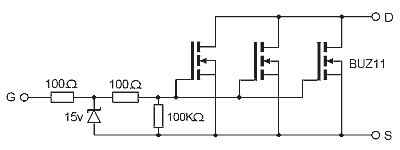
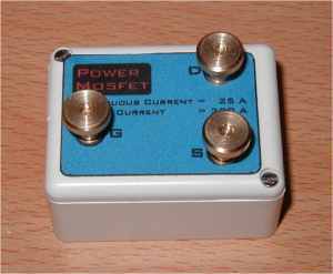
Power MOSFET Module A power mosfet module basically consists of a core mosfet and some additional protection components. There is usually a zener voltage clamp placed across the gate-source and drain-source terminals. The zeners protect the device from overvoltages between any of its terminals. The whole lot is self contained in a package with screw terminals and mounting lugs. While these are tempting devices they are also expensive so from a budget experimenters point of view I had to make my own. The core components
of this module are BUZ11 discrete power mosfets. These devices can conduct about
30A continuous with pulsed currents of around 130A. This may seem quite impressive
for such a small device (T0220 package) but these are the maximum ratings and
require certain conditions be met in order to perform to these specifications.
The first thing to realise is that there is no way this device will carry 30A
without a substantial heatsink. If you take a look at the BUZ11 data sheet you'll
notice that the thermal resistance from the junction to the ambient air is about
60 C/W. This means that for every watt of dissipation there will be an increase
in junction temperature of 60 C. The device is rated to a junction temperature
of 175 C so taking the ambient air temp to be 25 C gives a temperature difference
of 150 C corresponding to a dissipation of 2.6W. Now the on-resistance is 0.04 The pulsed rating of the device depends on its junction thermal capacity. The energy dissipated in a short pulse will be limited to the maximum allowable junction temperature. The data sheet states the device will handle a 134A pulse for a duration of 300us at a 1.5% duty cycle. If a longer pulse is required then the current must be de-rated accordingly. The data sheet also provides a graph of the Safe Operating Area. This shows the current, voltage and time limits in which the device will function without being damaged. This module is intended to operate as a pulsed device running at a very low (~0.1%) duty cycle and so the continuous current issue is not of concern. I'm using a standard of 1ms for rating the pulsed operation of modules so the current needs to be de-rated to about 90A per device. This isn't the full story with regards to a parallel module, additional constraints are required due to the slight differences between devices. These differences cause uneven sharing of the current which can be particularly significant during turn on and turn of periods. The circuit diagram is shown below:
Fig 1. MOSFET module circuit.
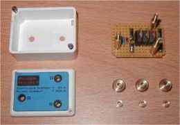
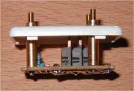
The connections are brought out through brass posts. These are threaded M3 so connections can be directly bolted on. With the mosfets contained in a closed package there is less risk of explosive shrapnel should the module fail. The module was constructed on strip board and the current carrying tracks were thickened with a heavy solder beading. For future modules I'll design a proper circuit board with heavy current tracks. The figures below show the various parts of the module:
|
|