|
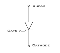
Switching Devices There are several broad categories of switching device available as listed below. The benefits and drawbacks of each type will be discussed briefly. 1. Thyristor (SCR) The thyristor is a three terminal device consisting of an anode, cathode and gate. The circuit symbol is shown below.
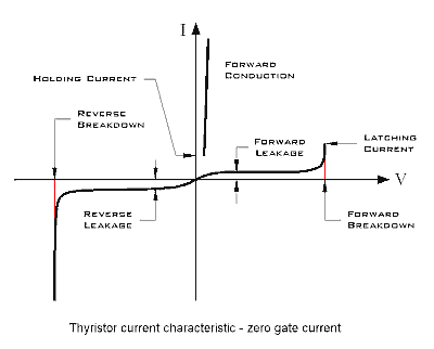
Fig 1.1 When there is no gate current the device is in the non-conducting state and will hold off positive and negative bias voltages. The zero gate current characteristic is:
Fig 1.2 If gate current is now injected into a positively biased device it will begin conducting current. Once the threshold latching current level is achieved the gate current can be removed and conduction will continue. The device will remain on until the anode current is reduced below the the holding current. The latching current and holding current levels are not the same. This is the device of choice when using a basic capacitor discharge coilgun. The thyristor will hold off the capacitor voltage until it is triggered into the forward conduction zone by the gate current signal. The capacitor then discharges through the thyristor into the coil and the current decays to zero. There is no option for turning off the the current once the device is conducting.
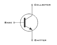
2. Bipolar Transistor: NPN This device operates as a current amplifier. It consists of three terminals, the Base, Emitter and Collector. Its circuit symbol is shown below.
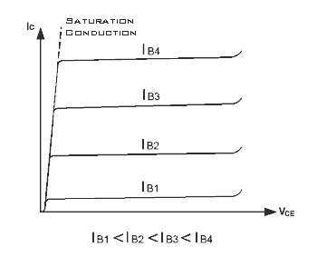
Fig 2.1 The device amplifies the current into the base terminal by allowing a much larger current to pass from the collector to the emitter. This gain varies between transistor types ranging from several hundred for small signal transistors to a few tens for high current power transistors. When used as a switching device the bipolar transistor is operated in saturation mode as shown below.
Fig 2.2 When the device is saturated the voltage drop across the collector and emitter is minimised, and consequently so are the conduction losses. You need to supply a large enough base current to ensure the device will be saturated at the required collector current. While bipolar power transistors offer high current capacity they require substantial base drive current (as much as 10% of the collector current in some cases) and this requires additional signal processing from the control system.
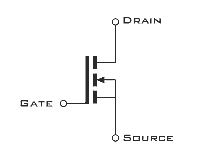
3. Power MOSFET: N-Channel Enhancement Mode The MOSFET is a three terminal device consisting of a source, drain and gate. The symbol is:
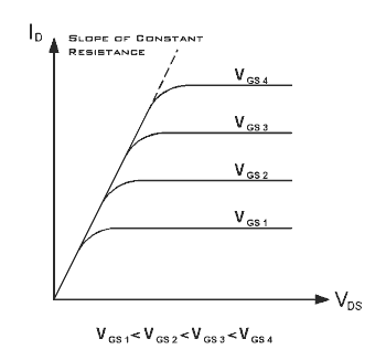
Fig 3.1 The current is controlled by the gate-source voltage level. A typical threshold voltage is around 2-3V above which the device begins to conduct. The diagram below shows typical current curves for various gate-source voltage levels.
Fig 3.2 This graph shows that the MOSFET behaves as a plain resistance over a certain range of drain-source voltages. The gate-source voltage controls the limit on the conduction current. For the purposes of simply current switching, the MOSFET should be operated within the constant resistance region. This means that for maximum current capacity the gate-source voltage should be pulsed at the correct value. If you take a look at a typical power MOSFET data sheet you'll find a set of current curves like those above. At higher gate-source and drain-source voltages the current has a more complicated characteristic.
4. Insulated Gate Bipolar Transistor This device offers the ease of control of the MOSFET with the higher current capacity of the bipolar transistor. The IGBT does require a slightly higher gate voltage to ensure that it is fully turned on. IGBTs are more difficult to operate in parallel due to their negative temperature coefficient.
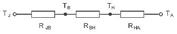
5. Semiconductor Thermal Issues - All devices have some form of conduction resistance and this leads to the generation of heat when the device is in operation. The ability to dissipate the heat is one of the major factors determining the operational voltage and current capacities of a device. The manufacturers of devices and heatsinks provide data about their dissipation capabilities and these allow us to correctly select components. The flow of heat starts at the semiconductor junction through which the current travels. Heat is conducted through to the device body to the casing surface and then to the air. If the device is fixed to a heatsink then there are two additional stages in the heat flow path. In order for the heat to flow there must be a temperature difference between each stage. We define the thermal resistance of a heat conduction stage by the ratio of the temperature difference and the power dissipation as shown below.
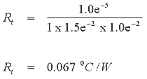
Lets look at the simple situation where we have a device with the following parameters:
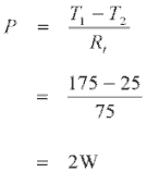
Table 5.1 We can use this data to calculate the maximum dissipation from the device operating without a heatsink Rearranging the eqn 5.1 for P and solving gives us
At this level of dissipation the continuous current would be restricted to 7A. Clearly the operation of the device is severely limited without the use of a heatsink. Suppose we want to run the device at its maximum continuous current, how do we select an appropriate heatsink?
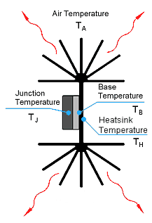
Fig 5.1 Firstly we need to examine the thermal resistance of a series of linked components. The diagram below shows the relationship between the thermal resistances and the temperatures at the interfaces.
Fig 5.2 The flow of heat through the various stages can be represented as a series connection of thermal resistances. What might not be so obvious is the value of the base to heatsink thermal resistance, RBH. This depends on the method used to fix the device to the heatsink. For most low voltage applications using a single device, simply bolting it directly onto the 'sink with some heat transfer compound smeared between the mating surfaces is fine. A typical value for the thermal conductivity of a heat transfer compound is around 1 W/mK (watts per metre - kelvin). To find a thermal resistance for this interface we need to take a closer look.
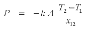
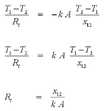
Fig 5.3 Power dissipation is related to the physical parameters by the formula
where k is the thermal conductivity, A is the interface area, T2 is the low temperature, T1 is the high temperature and x12 is the thickness of the interface layer. We can equate this to the thermal resistance formula above to get
Now the thickness of the heat conducting layer is of the order of say, 10um, the length and width of the package base is 15mm and 10mm respectively (we'll ignore the hole in the tab) so plugging these values into the eqn 5.3 gives us
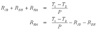
This is a very small thermal resistance and it's not surprising considering the wafer-thin layer of compound between the base and the heatsink. In many cases it's probably safe to ignore this completely. There are other methods of fixing devices to heatsinks which provide high electrical insulation by using a thin plastic backing piece and in these instances, the thermal resistance will more than likely need to be considered. Finally we can calculate the required heatsink thermal resistance as follows. Since the total thermal resistance is just the sum of the individual resistances we can write
The power dissipation will be 36W so plugging in the values we get
This requires a fairly meaty heatsink! Go look up a heatsink with this thermal resistance and you'll see what I mean. These issues are further complicated by the fact that the device resistance changes with junction temperature. Data sheets now tend to carry two current ratings for the device; one for 25 0C, and the other for 100 0C. The latter is a more realistic value to use when selecting a device.
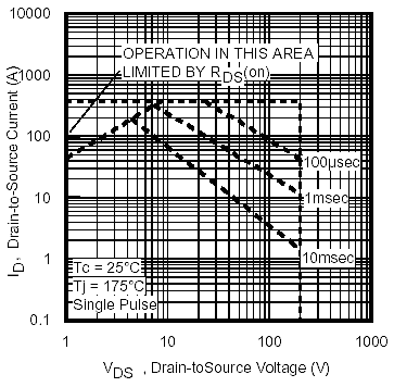
6. Pulsed Switching Issues- In pulsed switching applications such as the coilgun the switching and conduction losses determine the maximum operating current and voltage levels. The safe operating area, as defined in the device data sheet, details the current and voltage boundaries which will not damage the device. Fig 6.1 shows a typical Safe Operating Area characteristic.
Fig 6.1 IRFP90N20D Safe Operating Area
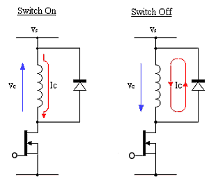
One thing which you should note is that the drain-source voltage limits are much more restricted at higher currents. The limiting slope on the left side of the graph is due to the devices resistance - the current rises linearly with the voltage. Dissipation within the device places an upper limit on the constant voltage and current that the device can handle. 7. Inductive Switching Issues- The switching of inductive loads can be very hazardous for the health of the switching device. While mechanical switches can cope with the arcing between the contacts at the expense of operating life, a semiconductor device will almost certainly be killed by the large voltage transient at turn off. The simplest method to solve this problem is to use a commutating or clamp diode across the inductive component. The diagram below shows the layout of a diode clamped coil with MOSFET switch.
Fig 7.1 When the switch is conducting, the diode is reverse biased and therefore no current exists in the diode branch. If the MOSFET is turned off quickly, the collapsing magnetic flux of the coil induces a voltage in the coil which tries to maintain the current. The faster the current is switched off, the larger is the induced voltage. Without a commutating diode the induced voltage could reach several hundreds or even thousands of volts - certain death for the MOSFET if the pulse exceeds the rated avalanche energy. Basically the commutating diode provides a low resistance path for the induced voltage to drive the current. The voltage only needs to rise enough to reach the conducting voltage of the diode, usually around 1V. This keeps the MOSFET happy and ready to fire another projectile. While this is certainly an effective means of limiting the turn off transient voltage, it isn't necessarily the best in terms of turn off speed. Ideally we want the current in the coil to turn off as quickly as possible. The simple commutating diode is far from this goal. If we want the current to decay faster we need to let the induced voltage reach a higher value. The absolute maximum we can allow it to rise depends on the voltage rating of the device. Suppose we are using a 60V MOSFET and a 40V supply, the largest induced voltage allowable is then 20V. One possibility is to connect a resistor in series with the diode. The specific value would need to be determine according to the coil current at turn off, the supply voltage, and the maximum device voltage. Another would be to use a zener voltage clamp across the MOSFET There is a whole area of semiconductor power electronics which deals with switching issues, the circuits are usually termed 'snubber' circuits.
|