|
Triggering Circuits There are three main methods of triggering available. Firstly there is what is termed open loop triggering. In this method the current is pulsed into the coil for a specific period of time and then extinguished. Trial and error is used to determine the best pulse period. This method encounters problems with its sensitivity to initial conditions, in particular the projectile position. This method is perhaps best used as a simple triggering system for a single coil where a user wants to experiment over a range of pulse widths and projectile starting positions. An extension of this method involves 'firing' a capacitor into a coil using an thyristor (SCR) device. In this case the relative performance depends on the capacitor, coil and projectile parameters. Secondly we have optical triggering. This type of system uses an infra red gate positioned at the 'input' end of the coil. As the projectile breaks the beam a signal triggers the switching device. The device remains triggered until the projectile passes the beam. Since we want the current to turn off just before the projectile passes midpoint this places an upper limit on the length of the projectile. At most the projectile length should be equal to the coil length. Thirdly there is induced voltage sensing. In this case a secondary sensing coil is wound round the drive coil. This sensing coil detects flux linkage changes and produces a voltage proportional to the rate of change of flux linkage. The induced voltage can be used as a triggering signal. The implementation of these methods is described in more detail below:
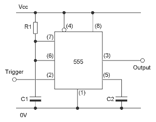
1. Open Loop Triggering - We will start by looking at a simple 555 timer circuit which can be configured to produce a range of pulse outputs. In this circuit the 555 is said to operate in 'one-shot' mode. The timing behaviour of the 555 is governed by a resistor and a capacitor. Take a look at the circuit in fig 1. In its non-triggered state the output pin (3) is low and discharge pin (7) is low. In this state capacitor C1 remains discharged. When a negative edge is applied to the trigger pin (2) the output goes high and the discharge pin goes into a floating state. C1 then begins to charge and when the voltage at the threshold pin (6) reaches 2/3VCC the output goes low. At this point pin (7) goes low and discharges C1. The device is now in its reset state. Pins (4) and (5) are not used in the functionality of this circuit. Pin (4) is the reset pin (active low). Pin (5) is the control voltage pin which is decoupled via a capacitor to ground.
Fig 1.1
Now the output pulse time tp is given by
This
equation arises from the time it takes the exponential RC transient to reach the
resetting voltage of 2/3 of the supply. If you solve the
general exponential growth function for a voltage of 2/3
max, the time solution will be 1.1 Note that the LOW signal to the trigger pin on the 555 must be shorter in duration than the output pulse width. You can make a trigger pulse circuit from common digital components. An excellent source of circuits for timing applications is Timer/Generator Circuits Manual by R.M. Marston.
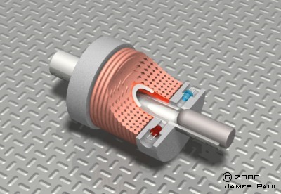
2. Optical Triggering - This is a highly versatile method since it provides precise triggering signals regardless of the particular coil or energy supply configuration. It is also largely immune to electromagnetic interference. The only possible pickup is in the wiring to the infra red gate. It is however crucial that the gate is working correctly when main power is switched on. If the optical gate fails then the switching device will be triggered and voltage will be applied to the coil until it either burns out or the supply is disconnected. Failure of the optical gate does not necessarily mean an electrical failure, for instance if the emitter or sensor becomes blocked by dirt then the system will produce a false trigger signal. The illustration below shows the physical arrangement of the emitter and sensor. In this configuration the slots along either side of the tube extend to the optical gate so that separate holes are not needed.
Fig 2.1
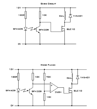
The most basic circuit consists of an emitter-sensor pair, a switching device and the coil. An improvement on the basic circuit involves some simple signal processing with an opamp. To avoid confusion I'll call the gate 'clear' when the beam is unbroken and 'blocked' when the beam is broken.
Fig 2.2
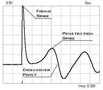
Let's consider the basic circuit. When the gate is clear the phototransistor SFH309 is conducting and the voltage at its collector is small since most of the voltage is dropped across the collector resistor. This is the voltage which controls the switching device, a mosfet in this case. Now when the gate is blocked by the projectile the phototransistor conducts very little current and so the voltage at its collector rises closer to the supply voltage. This turns the mosfet on and current passes through the drive coil. The projectile begins to accelerate into the coil and as it approaches the middle of the coil it clears the gate. The phototransistor now begins conducting again and the mosfet is turned off by the low collector voltage. The diode across the drive coil is known as a commutating diode. Its purpose is to reduce the voltage spike at the mosfet drain terminal when it switches off. The theory section on switching devices explains the issues of switching inductive loads. The second circuit is an improvement on the basic model. The opamp is being used as a comparator and the sensitivity of the circuit can be adjusted by changing the values in the resistor branch on the inverting input. The significant difference is that the opamp output can source and sink considerably more current than the phototransistor. This plays an important role when turning the mosfet on and off. In order to turn on the mosfet you have to establish a voltage at its gate terminal and this has a corresponding electrical charge associated with it. To turn off the device this gate charge must be removed. How quickly the charge can be established and removed dictates the switching speed. The opamp offers a current source/sink of lesser resistance than the phototransistor and so it produces a faster turn on/off. 3. Induced Voltage Triggering - This sensing method seeks to make use of the dynamic magnetic flux associated with the drive coil and projectile. If we look at the voltage induced in the sensing coil we can see how this waveform can be used in a triggering circuit. The graph below shows an induced voltage waveform. The trace resulted from turning on the drive coil and letting the projectile oscillate back and forth in the tube. This method is more suited to a constant voltage source supply since large transients in the supply will cause problems with the definition of the turn off point. We are only interested in the early part of the curve.
Fig 3.1
The problem with implementing induced voltage triggering is that of tuning. The relationship between induced voltage and projectile position depends on many interacting variables so the setup will require some trial and error to achieve optimal trigger timing. This is under development.
Last Modified: 12 Feb 2004 |