|
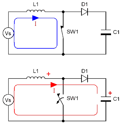
Electromagnetic Pistol: CS-P01A Voltage Converter Design 1 The two most important considerations for this system are that the component count and occupied volume should both be low. One system that fulfills these requirements is the boost converter. A boost converter employs an inductor, a switching device, and an output diode to generate pulses of current at elevated voltage. The basic circuit is illustrated in fig 1.
Fig 1. Principle of boost converter operation.
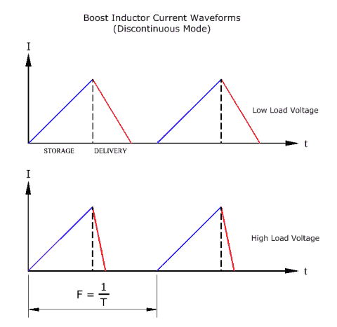
The circuit operates as follows: When the switch is closed a current is developed in the inductor which increases according to the time constant of the circuit, this is termed the storage phase. The switch is then opened after some small period of time and this causes the voltage across the switch to increase as the inductor's collapsing magnetic field attempts to maintain the current. Since the switch effectively becomes an open circuit, the voltage continues to rise until current is conducted through the output diode. Current is driven through the diode until the energy that is stored in the inductor is expended, this is termed the delivery phase. Since the inductor can effectively boost the supply voltage by a factor of 10-15 it is possible to charge high voltage capacitors from a low voltage battery source. The operating frequency of this type of device can be anywhere between 50-250kHz so the diode and switch must be capable of fast, efficient switching. A standard rectifier diode and bipolar transistor would not be the ideal components in this regard, although the circuit should still function at lower frequencies. The current waveform in the inductor will depend on the nature of the load to which it is connected. A capacitor load behaves very much like a constant voltage on the timescale of a storage/delivery cycle so the current ramps down more or less linearly during each delivery phase. As the capacitor voltage increases the delivery phase current ramps down faster due to the larger inductor induced voltage. Note that as well as the inductor's stored energy, the source (Vs) also supplies energy during the deliver phase. This energy is the time integral of the source power output during this phase, and it decreases as the load voltage increases (the current ramps down faster so the time that the source delivers power also decreases). Fig 2 illustrates what the waveforms would look like.
Fig 2. Typical current waveforms.
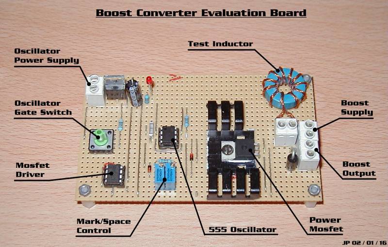
In order to develop a useful embodiment of the boost converter, an evaluation board was built in which the performance of test inductors could be determined over various operating conditions. Fig 3 shows the circuit board. Click on the image for a detailed diagram.
Fig 3. Boost converter evaluation board.
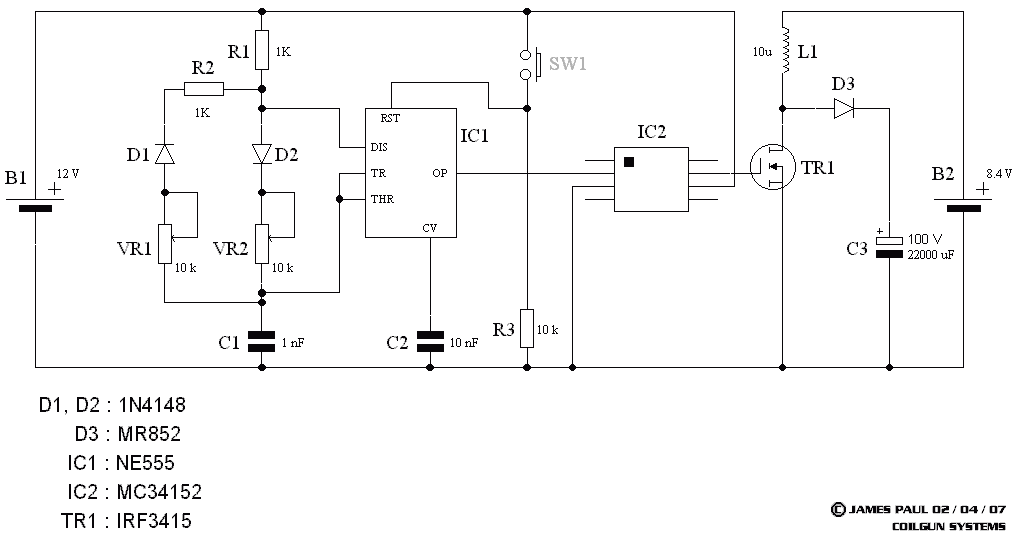
The circuit diagram is given in fig 4. Click on the diagram for a larger version.
Fig 4. Boost converter evaluation circuit.
The oscillator and MOSFET driver (IC2) are powered from the same 12 V source for the sake of convenience. While the oscillator could run from 5 V upwards, the MOSFET driver really needs a 12 V supply to ensure that it switches the MOSFET fully on during each cycle. The mark and space time periods are independently variable by adjusting VR2 and VR1 respectively. The typical operating frequency for this circuit was 100 kHz. The oscillator is held in an off state until SW1 is closed, it then operates until SW1 is opened again. The boost converter section is powered from a separate 8.4 V @ 900 mAh NiCd battery source. Note that the boost converter has the potential to continue charging the capacitor until something breaks down. It's possible to add an automatic gating facility to the oscillator such that the boost converter stops charging when a preset voltage level is achieved. This feature will be incorporated into the pistol control system. The time, T, taken to charge a capacitor to a specific voltage, Vc, can be estimated from the following formula -
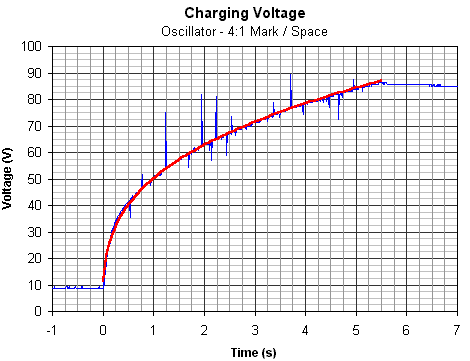
where C is the capacitance, Vs is the supply voltage, n is the delivery phase efficiency, f is the operating frequency, L is the inductance, and I is the inductor current at switch turn off. The reason for including Vs in the equation is that the capacitor initially charges to this value through the diode when the supply is connected. Note that this equation assumes that the inductor current starts and ends at 0 during each cycle. This condition depends on both the mark/space ratio and the output/input voltage ratio so the equation is a rough guide. It also ignores the energy delivered by the source during the delivery phase. This is reasonable if most of the charging occurs with a large load voltage (say, Vload > 4Vs). Something else to consider is that a boost converter generates quite a lot of EMI due to the rapid inductive switching (something which is very apparent if you've got an AM station playing on a radio). It is therefore necessary to pay attention to the layout of the circuit board so as to avoid nasty noise coupling into the oscillator and messing it up. There are ways of reducing the EMI which involve controlling the turn off time of the MOSFET. An example of the charging behaviour is given in fig 4. Note the large spikes present in the voltage waveform - a clear example of the EMI being picked up by the 'scope.
Fig 4. Charging voltage on stage 2/3 capacitors.
|