|
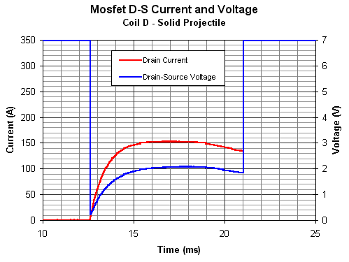
MOSFET Switching Results Switching There are two main parameters which need to be addressed when considering the efficiency of a switching device, these are the switching losses and the conduction losses. The switching losses arise during the turn-on and turn-off portions of the conduction waveform and are calculated by integrating the power dissipation (I*V) over the duration of these transient events. The conduction loss is simply the dissipation during the conduction part of the waveform and is also calculated by integrating the I*V function. Given the correct gate drive conditions mosfets can easily switch from the off state to fully on in less than a microsecond. Since the full conduction time in low power coilguns is of the order of 1-15ms we really only need to concern ourselves with the conduction losses. The conduction waveform for coil D as shown in fig 1.
Fig 1. Mosfet conduction waveforms.
The
first thing we can see from this data is that the switching time of the mosfet
is extremely fast compared to the total conduction time. The transition is so
fast that it requires the waveform to be captured with a microsecond timebase.
When the device is off the D-S voltage is sitting at the source level of 32V.
When the trigger pulse turns the device on the DS voltage collapses to 0V in much
less than 1ms and only begins to rise as current is conducted through the device.
In a similar way the DS voltage rapidly rises as the device is turned off. Notice
that the DS voltage waveform follows the shape of the current trace. This characteristic
shows the resistive nature of the mosfet. If we calculate the resistance of the
mosfet module based on the peak current and corresponding voltage we arrive at
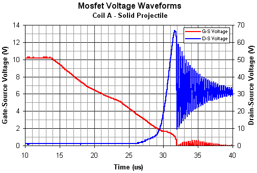
a value of 13m We can examine a typical G-S and DS turn off voltage waveform in a little more detail as shown in fig 2.
Fig 2. Turn off voltage waveforms for gate and drain terminals.
Looking at the G-S voltage we can see that it takes the opamp output about 18us to reduce the gate voltage to zero. Calculating the gradient of this line gives a slew rate of 0.53 V/us. Although the 358N data sheet doesn't specify an open loop slew rate, this value is similar to the slew rate recorded in the data sheet voltage follower pulse response graph. A slew rate of 0.5V/us is typical of general purpose opamps but something faster will be needed for high power coilguns - there are several options for fast gate drive circuitry which will be investigated in the future. If we look at the D-S voltage waveform we can see that the turn off transition begins at 26us and is complete at 32us - the end of the avalanche breakdown (see below) and the beginning of the oscillation. Now, the G-S voltage at 26us is just under 4V which is 1V greater than the 'typical' threshold voltage of 3V. The reason why the gate voltage can drop so low before the D-S voltage begins to rise is due to the low conduction current in each of the BUZ11 devices. In this coil A example the current at turn off is 19A so the current per device is only 6.3A. Data sheets sometimes contain a set of output characteristic curves which show the drain current as a function of D-S voltage for discrete values of G-S voltage. Looking at the Fairchild Semiconductor data sheet for the BUZ11 we find that the maximum drain current at a G-S voltage of 4V is 2.5A which is much less than the 6.3A calculated above. It's reasonable to ask why this difference exists and there are two explanations which come to mind. The first is that the devices might have lower threshold voltage than the typical value. The second is that the G-S voltage is being measured at the terminals of the MOSFET module which contains some 'protection' circuitry between the module gate post and the mosfet gate terminals. This means that, due to the gate capacitance, there could be a significant voltage drop across this resistor/zener network as the charge flows from the gate. Exploring the first possibility yielded a threshold voltage of about 3.2V so this explanation was abandoned leaving the protection network as the likely culprit. Some rough calculations using the gate charge and slew rate indicated that there would be about 0.5V dropped across the network. This would mean that, at the turn off transition, the actual voltage at the mosfet gate would be about 4.5V with a corresponding current of 6A per device and a total current of 18A. This is in much better agreement with the actual current level. It might be worthwhile to investigate this further from a measurement standpoint. This is an important lesson in realising that you might not be measuring exactly what you think you're measuring. This will make me pay more attention to the measurement layout in future.
MOSFET Module BUZ11 RIP. The threshold voltage measurement involved determining when a 'significant' current was conducted through the module. Unfortunately this current became too significant and coupled with the 32V across the D-S was enough to cook the BUZ11s before I realised what was happening. Replacing the mosfets only requires a bit of desoldering and this is actually a good opportunity to substitute the BUZ11s for BUZ22s. These devices are rated at 100V so I'll be able to use the module for some 'intermediate' voltage capacitor experiments.
Avalanche Breakdown Another device attribute of interest is the ability to 'absorb' voltage transients. Most modern mosfets are designed to cope with a limited degree of avalanche breakdown through the D-S path, these are described as 'avalanche rugged' or 'avalanche rated' devices. The limiting factor governing this breakdown is the junction temperature rise due to energy dissipation. Using this ability it's actually possible to drive inductive loads such as solenoids without the need for a clamping or commutating diode. Unfortunately this is not the case in a coilgun simply because the amount of energy stored in the field at turn off is too large to be dissipated during avalanche breakdown - the device junction would be cooked. The avalanche breakdown capability is, however, still useful in a coilgun context. If the coil is clamped with a standard rectifier diode there can still be a large short term voltage transient at turn off due to the slow reverse recovery of the diode. Normally a RC snubber or zener diode could be connected across the D-S terminals in order to absorb the transient until the diode recovers. However these are not needed if the transient energy is within the devices avalanche capacity. A 'small' snubber may still be fitted to remove the ringing which occurs after the diode begins conducting. Fig 3 shows the turn off transient current and voltage (the test circuit used a small snubber).
Fig 3. Avalanche transient waveforms
If we look at the D-S voltage we can see that it exceeds the rated 50V by about 20V for a total duration of around 8us. This period represents the device under avalanche breakdown. At the end of the breakdown the D-S voltage drops to just below 50V at which point the commutating diode(s) takes over. During breakdown the current through the D-S path decays and, interestingly, it goes negative before finally returning to zero. I'm not quite sure why this happens but it could be due to stray inductance in the current sensor - a redesign may be needed for measuring microsecond events. The data sheets illustrate the current stopping when it first reaches zero but it might due to either the commutating diode or mosfet body diode recovery mechanisms. The negative current is not a consequence of the snubber since it occurs with or without the snubber. If the D-S current and voltage are multiplied we can plot a power dissipation curve for the breakdown. If this curve is integrated then the avalanche energy can be calculated. Since I'm not sure why the current goes negative I'll ignore this portion of the waveform and determine the energy dissipated up to this point. Importing the data into Matlab and using the trapezium integration function yields a value of 15.2mJ. This is energy is dissipated in only one device because it is ver unlikely that the devices will have closely matched avalanche voltage levels. Even so, this energy is within the 200mJ 'cold' junction avalanche capacity of the BUZ11. Obviously the junction isn't going to be cold after conducting a large current pulse and the better data sheets (many don't) provide enough information on the avalanche characteristics to enable us to make an estimation of the allowable avalanche energy. |
|