|
Induced Voltage Sensor Delta-Peak Trigger
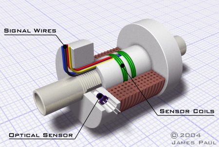
Induced voltage triggering is an alternative method of providing closed-loop control of the coil current in single-stage or multi-stage transistor-fired coilguns, or pseudo closed loop control of the current in multi-stage thyristor-fired coilguns. The induced voltage trigger signal is used to turn off the current on the active coil and initiate the discharge through the next coil (if there is one). This is why it is unsuitable for use with single stage thyristor fired coilguns - the turn off functionality is superfluous. The main reason for pursuing this method is that it should be possible to employ it in very high power coilguns where the components of a directly integrated optical trigger might be damaged by the intense, rapidly changing field. That said, the optical trigger could be coupled to the coilgun via fibre optic links, thereby eliminating the potential for device damage, although this does add a layer of complexity. Various induced voltage sensor setups were designed and tested in order to determine a suitable triggering point on the induced voltage waveform. An optical trigger was incorporated into the test coils so that this known turn off point could be used as a reference for the induced voltage waveform. Initial designs attempted to minimise the effect of flux linkage changes associated with the coil current by utilising two closely spaced sensor coils connected such that their voltages cancelled when the coil was dry fired. This approach was based on two ideas; that the firing spike was an undesirable signal feature, and the potential for external magnetic fields to cause problems would be reduced by using closesly spaced sensors. The problem with this approach was that with the projectile located at its launch position in the coil, the resulting asymmetry made it very difficult to trim out the firing spike. The separation of the sensors was also investigated but there was no waveform feature close to the optical trigger turn off point that would be useful for triggering purposes. Fig 1 shows an example of a test coil* with closely spaced sensors positioned centrally along the drive coil axis. The inclusion of the former for holding the sensor windings significantly increases the inner radius of the drive coil, thereby adversely affecting the performance. Using a very fine wire would reduce the necessary radial displacement but, as mentioned above, the lack of a suitable trigger feature on the waveforms ended any further investigation of this design.
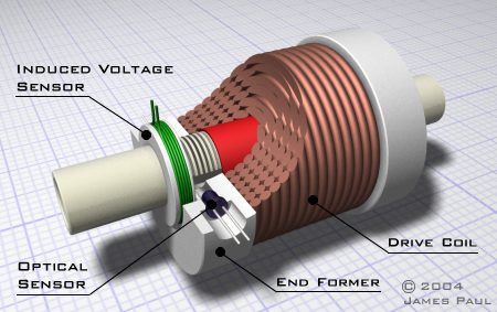
Fig 1. Dual sensor coil At this point it was decided that FEMM simulations would be a more productive means of determining sensor voltage waveforms in relation to projectile position. An example is outlined in Determining Induced Voltage Signals Using FEMM. Fig 2 shows the final design of the test coil based on results from several FEMM simulations. An optical sensor is included for trigger point verification and this forces the sensor coil to a location where it triggers off the current earlier than the optical sensor.
Fig 2. General layout of functioning test coil.
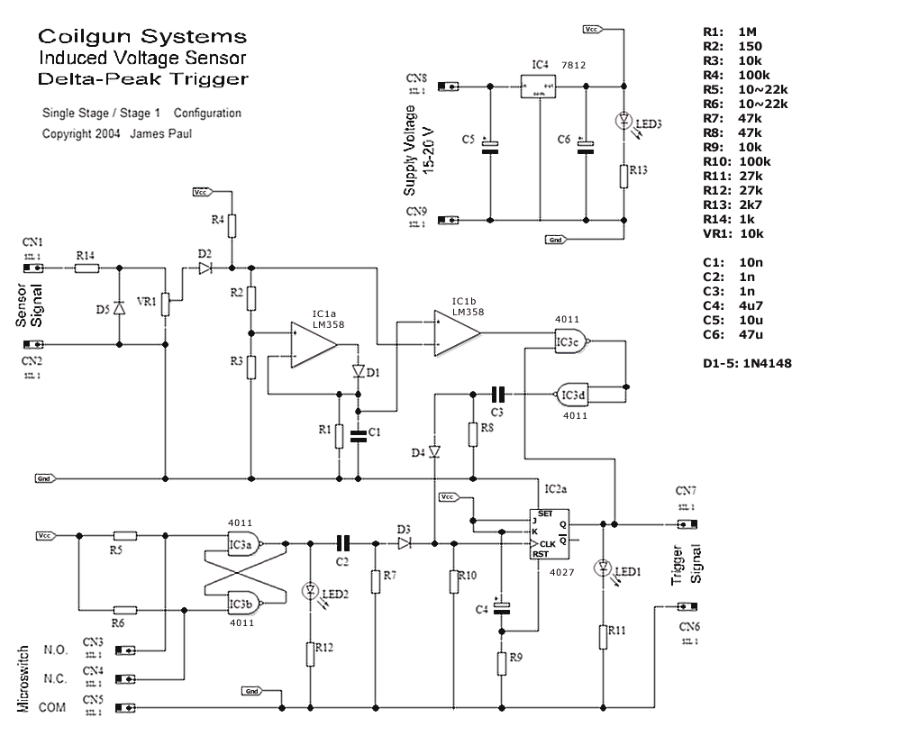
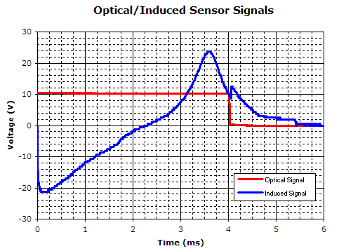
Single Stage Trigger Circuit Referring to the circuit of figure 3, let us consider the condition when the circuit has just powered up: The op amps are DC biased such that the output of IC1b is low. The J-K flip flop is configured such that positive transitions on the CLK pin cause the Q output to flip state. The power up default for Q is LOW. There are two capacitively coupled signal routes to the CLK input of the flip flop which are isolated from each other by signal diodes. The firing signal comes from a debounced microswitch (the firing switch), and the turn off signal comes from the op amp delta-peak detector. The delta-peak detector cannot trigger the CLK pin while the Q output is LOW. When the microswitch is pressed: The output of the debounced logic goes HIGH and a short pulse appears at the CLK pin. The Q output of the flip flop goes HIGH triggering the switching device and initiating the capacitor discharge into the drive coil. The negative induced voltage associated with increasing sensor flux linkage (the firing / penetration spikes) is clamped by the sensor signal rectifier diode. As the sensor flux linkage begins to decrease due to the passage of the projectile, and to a lesser extent, the natural decay of the coil current, the sensor voltage becomes positive. The rate of change of flux linkage increases to a maximum and then begins to decline as the rear of the projectile passes the sensor, resulting in a voltage peak. A scaled analogue of this maximum voltage is temporarily stored on C2 (the charge decays through R1) such that the output of op amp IC1b goes HIGH when the signal voltage drops slightly below its peak. The speed of the output transition from IC1b is too slow to generate a sufficiently short, capacitively coupled CLK pulse, therefore some logic gates are employed to sharpen the edge, as well as provide 'sensor lockout'. On receiving the second CLK pulse Q transitions to LOW and the switching device is turned off. Note that since Q is now LOW, no further sensor signals can toggle the flip flop. This dependency on the output state of Q is necessary in order to prevent double triggering which can occur when the coil is turned off. Double triggering is caused by a secondary sensor peak brought about by the rapid increase in the di/dt decay rate as the current is turned off. This secondary peak is detected and results in Q being set HIGH again. Since the projectile has passed the point of maximum rate of change of flux linkage there is no further voltage peak from the sensor, therefore the capacitor completely discharges into the coil. The use of this circuit is not limited to induced voltage sensors. Any sensor that produces a falling edge at the point where the current should be turned off can be used. It is possible to use an optical sensor with this circuit where the output of the optical sensor falls as the rear face of the projectile passes by. Fig 4 shows a typical sensor signal with the coil current being controlled by an optical trigger. The sensor peak occurs before the optical trigger output falls resulting in what might+ be a premature turn off. The sensor position is limited by the inclusion of the optical trigger, however there is no reason why the induced voltage sensor cannot be positioned more favourably in a 'production' coil. Note the occurrence of the second peak which coincides with the coil current being turned off. This secondary peak occurs much closer the primary peak when the current switching is controlled by the delta-peak trigger. It is interesting to note that in fig 4 we see no distinction between firing and penetration spikes with this sensor setup. The main reason for this is that the sensor used to generate the oscillogram in the link above was located centrally along the coil axis. Since the projectile takes some time to accelerate towards the sensor there is a lag between the firing spike and penetration spike making them distinct.
Fig 3. Delta-peak trigger circuit (click for large version)
Fig 4. Induced voltage sensor signal showing secondary peak at turn off.
Further investigation will look into the cascading of trigger stages for use with multistage coilguns. *Note the grooved region on the tube surface - this provides a good key for the epoxy which fixes the formers to the tube. Previous designs have used a simple roughened surface which has proven to be unreliable over time. +The effect of the turn off point on velocity and efficiency has yet to be investigated at the time of writing of this article.
Last Modified: 12 FEB 2004 |
|